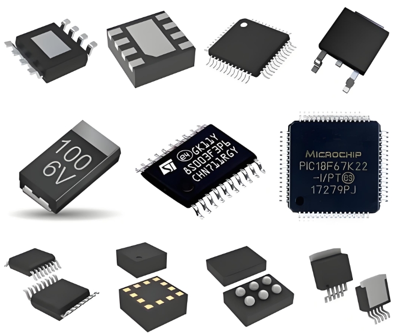
**AD9865BCP: A Comprehensive Technical Overview and System Integration Guide**
The **AD9865BCP** from Analog Devices is a highly integrated, mixed-signal front-end (MxFE®) processor designed primarily for broadband communications applications. This system-on-a-chip (SoC) combines a high-performance analog-to-digital converter (ADC), a digital-to-analog converter (DAC), and additional signal processing circuitry, making it an ideal solution for transceiver designs in systems such as **wireless local loops (WLL)**, cable modems, and power-line communications.
**Architectural Overview and Key Features**
At its core, the AD9865BCP architecture is built to handle both the transmit (Tx) and receive (Rx) paths with exceptional efficiency.
* **Transmit Path (DAC):** The chip features a **12-bit, 128/64 MSPS Tx DAC** with an integrated interpolation filter. This filter allows for a lower data input rate, which is then upsampled to the DAC's update rate, significantly simplifying the digital interface and reducing processing load on the accompanying digital processor (e.g., an FPGA or DSP). A programmable digital modulator allows direct conversion of the complex baseband signal to an IF frequency, a critical function for many modem designs.
* **Receive Path (ADC):** On the receive side, it incorporates a **12-bit, 64 MSPS ADC** with outstanding dynamic performance. The ADC is preceded by a programmable gain amplifier (PGA), which provides essential flexibility to accommodate a wide range of input signal levels. This ensures the ADC operates at its optimal range, maximizing the signal-to-noise ratio (SNR) for the entire system.
* **Auxiliary ADC and Control:** A secondary, lower-speed 12-bit auxiliary ADC is available for system monitoring tasks, such as **RSSI (Received Signal Strength Indication)** or power amplifier (PA) output power control. The device is configured via a flexible serial peripheral interface (SPI), allowing for precise control over its numerous settings, including power-down modes for reduced consumption in portable applications.

**Critical Considerations for System Integration**
Successfully integrating the AD9865BCP into a system requires careful attention to several key areas:
1. **Clock Generation and Distribution:** The performance of both the ADC and DAC is **highly dependent on the quality of the clock source**. A low-jitter clock is absolutely mandatory to achieve the specified dynamic performance. The clock input should be treated as a sensitive analog signal, with proper termination, isolation from digital noise, and use of a dedicated clock generator IC for best results.
2. **Power Supply and Decoupling:** As a mixed-signal device, the AD9865BCP demands a meticulous power supply design. **Separate analog and digital power domains (AVDD, DVDD)** must be provided and carefully isolated. Aggressive and strategic decoupling is non-negotiable; place a combination of bulk, ceramic, and high-frequency capacitors as close as possible to all power pins to minimize supply noise and prevent digital switching noise from corrupting sensitive analog sections.
3. **PCB Layout and Grounding:** A robust grounding strategy is paramount. A common practice is to use a **single, low-impedance ground plane** to avoid ground loops, while carefully partitioning the layout into analog, digital, and clock sections. Digital signals, especially the data and clock lines, must be routed away from analog inputs and the clock circuit. Proper impedance control for high-speed digital traces is also essential to maintain signal integrity.
4. **Interface with a Digital Processor:** The digital interface consists of data and control buses. It is crucial to ensure signal integrity by following standard high-speed digital design rules, including appropriate trace length matching and termination if necessary. The timing requirements detailed in the datasheet must be strictly adhered to for reliable data transfer.
5. **Filter Design:** The performance of the entire data chain is finalized by the external analog filters. On the Tx path, a reconstruction filter is needed to remove images from the DAC output. On the Rx path, an anti-aliasing filter is required to prevent out-of-band noise from folding back into the desired band. These filters must be designed to meet the specific requirements of the application's bandwidth and rejection needs.
**ICGOOODFIND:** The AD9865BCP stands as a powerful and highly integrated mixed-signal front-end solution that significantly reduces design complexity and board space for broadband communication systems. Its successful deployment hinges not just on its inherent capabilities but on a disciplined approach to system integration, with particular emphasis on power integrity, clock quality, and meticulous PCB layout to unleash its full performance potential.
**Keywords:** Mixed-Signal Front-End (MxFE), System Integration, Broadband Communications, Analog-to-Digital Converter (ADC), Digital-to-Analog Converter (DAC)
